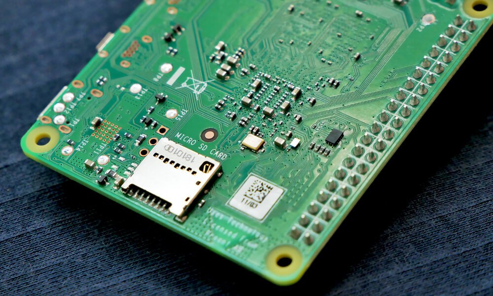
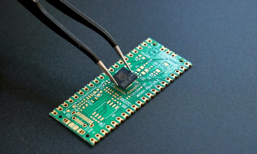
A Multilayer PCB (Printed Circuit Board) is a type of circuit board that consists of multiple layers of conductive material and insulating substrate stacked on top of each other. Unlike single-layer or double-layer PCBs, which have conductive traces on one or both sides of a single layer of substrate, multilayer PCBs have three or more layers of conductive traces and insulating material.
The layers in a multilayer PCB are bonded together under heat and pressure, often with the use of special adhesives. Electrical connections between layers are typically made through “vias,” which are small holes drilled through the layers and then plated with conductive material.
Key Features:
- Complex Circuitry: Enables the design of complex circuits in a compact space due to multiple layers for routing electrical traces.
- High Density: Allows for a high density of components and connections, making it ideal for advanced electronic applications.
- Improved Signal Integrity: Dedicated layers for power and ground planes can improve signal integrity and reduce electromagnetic interference (EMI).
- Enhanced Functionality: Capable of hosting multiple complex functions on a single board, which is beneficial for high-performance applications.
- Design Flexibility: Greater latitude in designing complex circuits and incorporating additional features.
Common Applications:
Multilayer PCBs are often used in applications that require high performance, compact size, and multiple functionalities, such as:
- Computer motherboards
- Smartphones
- Medical equipment
- Aerospace and military devices
- Industrial controls
- Networking equipment
Advantages:
Multilayer PCBs offer numerous advantages including higher component density, better signal quality, increased design flexibility, and improved reliability and durability. These benefits make them suitable for a wide range of high-end electronic applications.


